


EM-Tec FG1 silicon SEM finder grid substrate
Order # 10-008144 EM-Tec FG1 silicon SEM finder grid substrate
Introduction
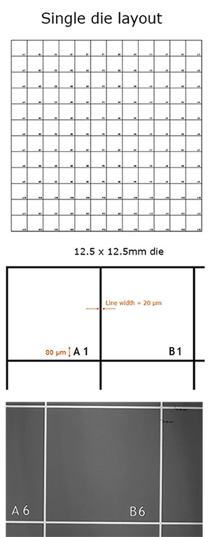
The EM-Tec FG1 silicon finder grid with 144 fields of 1x1mm has been designed to enable easy relocate small samples. The unique label in each field provide an exact reference and quick finding method for sample positions. It is intended for:
- correlative, corroborative, collaborative and repetitive microscopy
- multi-sample mounting for small samples
- demonstration samples with quick finder grid
- quick size estimation with the 1mm grid
EM-Tec FG1 Construction
The EM-Tec FG1 silicon finder grid comprises an ultra-flat conductive silicon substrate with deposited chromium lines. The chromium lines are 75nm thick and 20µm wide. The chromium lines form excellent contrast for SEM imaging and reflected light microscopy. The 12.5 x12.5 mm die is divided into 144 fields of 1x1mm. Each field has a unique alphanumeric chrome deposited label of 80µm height in the lower right corner. Thickness of the substrate is 675µm.
EM-Tec FG1 specifications
Parameter |
Specification |
Pattern size |
12 x 12mm |
Field size |
1 x 1mm |
Number of fields |
144 |
Labeling |
Unique, alphanumeric |
Pattern lines |
75nm chromium, 20µm wide |
Labels |
75nm chromium, 80µm height |
Die (substrate) size |
12.5 x 12.5mm |
Orientation |
<100> |
Type |
P (Boron) |
Resistance |
1-10 Ohm/cm |
Grade |
Prime / CZ Virgin |
Coating |
None, native oxide only |
Thickness |
675µm (± 20µm) |
TTV |
≤1.5µm |
Warp |
≤30µm |
EM-Tec FG1 advantages
The EM-Tec FG1 silicon SEM finder grid substrate is a superior alternative compared to traditional copper SEM finder grids and engraved stubs. Advantages are:
- excellent planarity with ultra-flat substrates (no height difference as with copper finder grids)
- pattern is easily visible with SEM, light microscope and unaided eye
- each individual field is referenced with a unique label
- low background signal for SEM imaging (similar to Si chips)
- fine bright pattern over entire area (finer and clearer than laser engraved patterns)
- sample size can be easily judged against the 1x1mm fields
- compatible with Ø12.7mm pin stubs, Ø12.2mm JEOL stubs and Ø15mm Hitachi stubs
- easy to mount on SEM stubs and AFM/SPM discs
- reusable, solvent resistant and plasma cleaning compatible
Suggestions for using the EM-Tec FG1
Mount the FG1 silicon substrate on a suitable SEM stub with a conductive silver or nickel paste (EM-Tec AG42 or EM-Tec NI41).
Use a magnifier or low magnification stereo microscope to mount the samples.
Use small amount of conductive paste to secure the samples.
Record the positions(s) of the sample(s).
Place the SEM stub with the FG1 finder grids and mounted samples in the SEM.
Align the pattern with the X/Y movements of the SEM stage.
Relocate the sample(s) using previous recording notes.
Image sample and use same alignment if imaging with different microscope is needed.
Judge sample size against pattern if needed.
TSB 10-008144 EM-Tec FG1 silicon SEM finder grid substrate Revision 1