


Silicon wafers, substrates and sample supports
Silicon wafers, substrates and sample supports
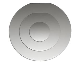
Si wafers: 51mm, 100mm and 150mm diameter
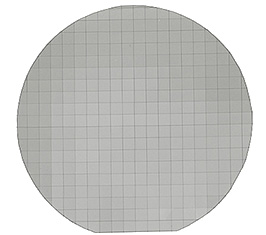
Diced silicon wafer
Introduction
Polished silicon is an excellent substrate for imaging, experiments, nanotechnology and micro-fabrication applications. It is available in the form of wafers, diced wafer or as smaller chips (pieces). The silicon wafer and chips all have a <100> orientation. Cleaving of the wafers to the desired size with a <100> orientation wafers is straight forward and simple. The silicon wafers and chips are all P-type, doped with B to provide excellent conductivity for SEM, FIB and STM applications.
For biological applications silicon resembles glass, which makes it a suitable support for growing and/or mounting cells. For imaging applications, it is an ideal sample substrate for small particles due to the low background signal of the highly polished surface.
Two grades of silicon substrates are offered:
- Micro-Tec standard silicon wafers and silicon chips for standard application and medium resolution imaging.
- Nano-Tec ultra-flat silicon wafers and ultra-flat silicon chips for demanding applications and high resolution imaging.
Micro-Tec <P/100> standard silicon wafers and diced wafer for SEM substrates
The Micro-Tec <P/100> silicon wafer substrates can be used for sample substrates, micro-fabrication, substrate for thin film research or biological substrates. Useful flat substrate for SEM imaging of particles due to the low background. For biological applications, Si has similar properties as glass and can be used to mount or grow cells. Can be easily cleaved or used as a whole wafer. The Micro-Tec Si wafers are packed in a wafer carrier tray for protection. The 100mm diced wafers are supplied on wafer adhesive disc and packed between two plastic sheets for protection. The Si chips can be easily lifted off the adhesive sheet. Sizes of the Si chips are 5 x 5 mm, 7.5 x 7.5 mm and 10 x 10 mm. De Si chips can be easily fitted to SEM stubs.
The Micro-Tec standard silicon wafer substrates are available as:
- Ø2”/51mm <P/100>silicon wafers
- Ø4”/100mm <P/100>silicon wafers
- Ø6”/150mm <P/100>silicon wafers
- Diced Ø4”/100mm <P/100>silicon wafer in 5x5mm chips (~270 pieces)
- Diced Ø4”/100mm <P/100>silicon wafer in 7.5x7.5mm chips (~112 pieces)
- Diced Ø4”/100mm <P/100>silicon wafer in 10x10mm chips (~55 pieces)
Parameter |
Ø2”/51mm wafer |
Ø4”/100mm wafer |
Ø6”/150mm wafer |
Diced Ø4”/100mm |
Diced Ø4”/100mm |
Diced Ø4”/100mm |
|
Product # |
|||||||
Orientation |
<100> |
||||||
Type |
P (Boron) with one primary flat |
||||||
Resistivity |
1-30 Ohm/cm |
||||||
Coating |
None, native oxide only |
||||||
Thickness |
275µm (+/- 20µm) |
525µm (+/- 20µm) |
675µm (+/- 20µm) |
525µm (+/- 20µm) |
525µm (+/- 20µm) |
525µm (+/- 20µm) |
|
Diameter |
51mm |
100mm |
150mm |
100mm |
100mm |
100mm |
|
Chip (die) size |
n.a. |
n.a. |
n.a. |
5x5mm |
7.5x7.5mm |
10x10mm |
|
Chip quantity |
n.a. |
n.a. |
n.a. |
~270 |
~112 |
~55 |
|
TTV |
≤ 20µm |
||||||
Primary flat |
15.9 +/- 1.65mm |
32.5 +/- 2.5mm |
57.5 +/- 2.5mm |
32.5 +/- 2.5mm |
32.5 +/- 2.5mm |
32.5 +/- 2.5mm |
|
Surface roughness |
<1.5nm, polished on one side |
||||||
Nano-Tec ultra-flat <P/100> silicon wafers and ultra-flat silicon chips
The Nano-Tec, ultra-flat P<100> silicon wafers have higher specifications than the Micro-Tec silicon wafers. They are preferred for demanding applications in micro-fabrication, as substrates for thin film research or biological substrates. Excellent ultra-flat surface for high resolution SEM imaging of particles due to the low background signal. For biological applications, Si has similar properties as glass and can be used to mount or grow cells. The larger wafers with the <100> orientation can be easily cleaved to the desired size. The ultra-flat Nano-Tec Si wafers are clean-room packed in a wafer carrier tray for protection. The ultra-flat Si chips are precision diced with a dicing saw, cleaned and clean-room packed in a gel-box. They can be easily lift off the gel substrate with flat tipped tweezers.
The Nano-Tec ultra-flat silicon wafers are available as:
- Ø4”/100mm <P/100> ultra-flat silicon wafers
- Ø6”/150mm <P/100> ultra-flat silicon wafers
- Ultra-flat 5x5mm Si chips; 25 packaged in a gel box
- Ultra-flat 5x5mm Si chips with 200nm thermal SiO2; 25 packaged in a gel box
Parameter |
Ø4”/100mm wafer |
Ø6”/150mm wafer |
5x5mm chips |
5x5mm chips with thermal SiO2 |
Product # |
||||
Orientation |
<100> |
|||
Type |
P (Boron) with one flats |
|||
Resistivity |
1-10 Ohm/cm |
|||
Grade |
Prime / CZ Virgin |
|||
Coating |
None, native oxide only |
Thermal SiO2 |
||
Thickness |
525µm (+/- 20µm) |
675µm (+/- 20µm) |
||
Diameter |
100mm |
150mm |
150mm |
150mm |
Chip size |
n.a. |
n.a |
5x5mm |
5x5mm |
Chips quantity |
n.a. |
n.a. |
25 |
25 |
TTV |
≤1.5µm |
|||
Bow |
≤30µm |
|||
Warp |
≤30µm |
|||
Primary flat |
32.5 +/- 2.5mm |
57.5 +/- 2.5mm |
||
Surface roughness |
Typically 0.2- 0.3nm, polished one side |
|||
Ordering Information for Silicon Wafers & Chips
|

|

|

|

|
|
|

|

|

|
